Google TPU 8tx and TPU 8i Max: two new eighth-gen systems for confidential inference and massive context
Google announced on Monday morning two new additions to its eighth-generation TPU lineup: TPU 8tx, built for confidential inference, and TPU 8i Max, a dual-chip package for massive context windows. It is the first time Google has introduced four TPU systems in a single year — and both newcomers are systems, not new chips, assembled from silicon Google already ships.
What we checked: Google’s official blog post “Introducing TPU 8tx and TPU 8i Max” (November 9, 2026), cross-checked against Reuters’ report the same day.
- What: TPU 8tx and TPU 8i Max, the third and fourth eighth-generation TPU systems, announced November 9, 2026.
- First: Google says it is the first time it has introduced four TPU systems in a single year.
- TPU 8tx: Same silicon as TPU 8t, paired with 5th Gen AMD EPYC hosts. Hardware confidential compute keeps data and model weights protected while in use, with up to 2× lower latency than TPU 8t.
- TPU 8i Max: Two TPU 8i chips in one package — double the compute, double the SRAM, and double the HBM bandwidth of TPU 8i.
- Baseline: TPU 8i pairs 288 GB of high-bandwidth memory with 384 MB of on-chip SRAM. The 8t/8i pair delivers up to 2.7× better training performance and 80% better inference price-performance than the previous generation.
- Availability: No price or date from Google; Bloomberg reported both systems due in 2027. Nearly 100 customers now run on TPUs.
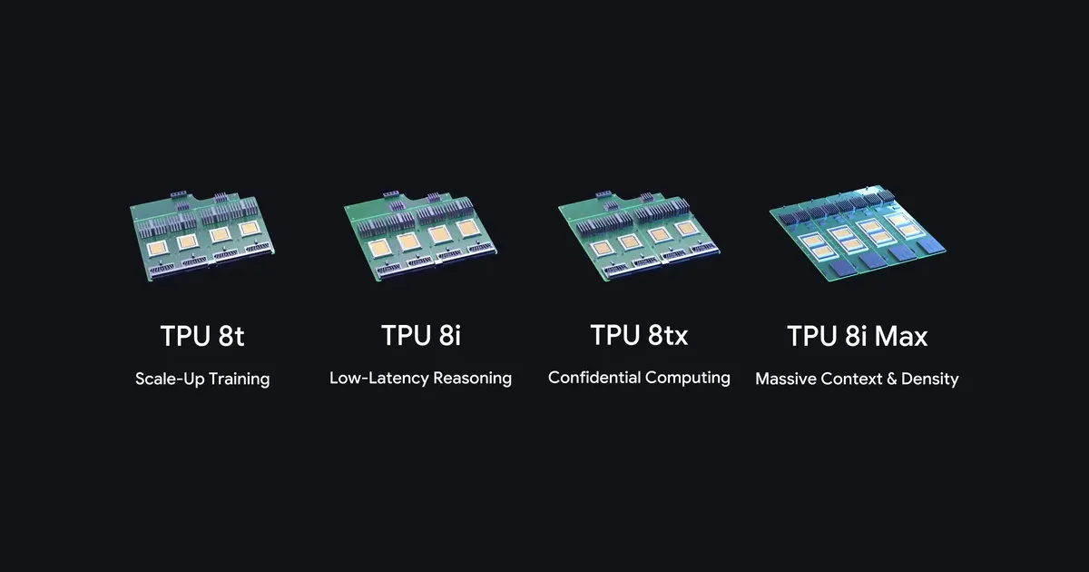
| System | Built for | Silicon and packaging | The number that matters | Status |
|---|---|---|---|---|
| TPU 8t | Large-scale training | Eighth-generation silicon | Up to 2.7× better training performance vs the previous generation | Available since April 2026 |
| TPU 8i | Real-time reasoning | Eighth-generation silicon; 288 GB HBM, 384 MB SRAM | Inter-chip communication delays cut by up to half | Available since April 2026 |
| TPU 8tx | Confidential inference, small-scale training | Same silicon as 8t; 5th Gen AMD EPYC hosts; Boardfly network | Up to 2× lower latency vs TPU 8t | Announced Nov 9, 2026; due 2027 |
| TPU 8i Max | Massive context windows; highest compute density per rack | Two 8i chips in one package | 2× compute, SRAM, and HBM bandwidth vs 8i | Announced Nov 9, 2026; due 2027 |
TPU 8t: the training baseline
Google introduced the 8t and 8i together at Cloud Next in April, as the first two systems of the eighth generation. The 8t is the training powerhouse, built for massive foundation models and tuned for what Google calls “goodput” — the useful intelligence delivered per watt. Against the previous TPU generation, Google claims up to 2.7 times better training performance.
The same April launch put the 8t and 8i at the center of Google’s HPC push — the pair also powers the HPC setup Google showed at SC26 this week, alongside its Antigravity coding agent and AlphaEvolve. The 8tx and 8i Max extend that same generation rather than replacing it.
TPU 8i: the reasoning engine
The 8i is the reasoning engine, designed to break what Google calls the memory wall: it cuts inter-chip communication delays by up to half, and pairs 288 GB of high-bandwidth memory with 384 MB of on-chip SRAM. Google claims 80% better inference price-performance than the previous generation.
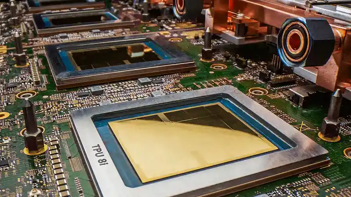
That memory-heavy design is why the 8i became the building block for today’s announcement. When the workload is a reasoning model juggling a long conversation, the bottleneck is moving data between chips, not the arithmetic itself — and the 8i was built to shrink exactly that delay.
TPU 8tx: the locked room
The 8tx answers a different customer: regulated enterprises and governments running frontier or proprietary models against their most sensitive data. Normally, data is encrypted at rest and in transit, but has to be unlocked in memory while a computer processes it. The 8tx builds security into the hardware layer, keeping sensitive data and model weights protected and isolated even while in active use.
It runs on the same silicon as the 8t, paired with 5th Gen AMD EPYC CPU hosts, and it borrows the low-latency Boardfly network Google built for the 8i’s real-time reasoning. The combination delivers up to 2× lower latency than the 8t, Google says, with a near-zero performance penalty. Because training-grade compute sits on the same system as the fast inference network, teams can fine-tune models on private data, distill large models into smaller ones, and train agents with reinforcement learning — all without migrating sensitive data between separate clusters.
It is the hardware answer to the same sovereign-AI demand driving NVIDIA’s Korea collaboration announced today: governments want AI that runs on their terms, on infrastructure they control, with their data never exposed in the clear.
TPU 8i Max: the memory answer
The 8i Max attacks the other bottleneck. When dozens of AI agents work together across an entire software codebase or hours of video at once, memory bandwidth becomes the limit. Google’s fix is blunt: take two low-latency TPU 8i chips and combine them onto a single package.
The result is double the compute, double the SRAM, and double the HBM bandwidth of a single 8i, so processors stay fed and large workloads don’t stall. And because the 8i Max fits twice the silicon within the existing rack footprint, data centers get significantly more computing power per square foot and per watt. It is the system for the agentic workloads Google keeps describing — agents reasoning across million-token contexts, not single prompts.
The software half of the announcement
Hardware was only part of Monday’s post. Google also pushed the software stack that makes TPUs usable by developers who don’t write TPU code: TorchTPU, open-sourced last month so PyTorch code and Hugging Face models run natively, with out-of-the-box backends for vLLM and SGLang; a TPU agent suite in preview that plugs into Claude Code, Cursor, and Antigravity to automate onboarding and kernel tuning; and the XLA Serving Engine for serving models from a low-latency C++ runtime.
Two pieces target agents specifically. The Agent Compute Engine automatically suspends idle agent sessions and shifts working memory off the chip in milliseconds, cutting infrastructure costs while agents wait on tools or humans. TPU Sync, now open-sourced, turns chip HBM, host DRAM, shared storage, and the network into a single memory hierarchy — Google claims it cuts KV transfer latency and time to first token by more than 90%. Cloud Pathways is now generally available on Google Kubernetes Engine, and GKE dynamic slicing, also generally available, claims up to 5× faster job startup and 4.5× faster fault recovery.
Google also points to industry-standard InferenceX and AgentX benchmarks, where its vLLM-TorchTPU stack achieved what it calls state-of-the-art price-performance. Those are Google’s own numbers on its own stack, not independent results — no third party has tested either new system yet.
The verdict
Read the announcement for what it is: packaging innovation, not new silicon. Google’s bet is that modularity — same chips, different packaging, networking, and memory — lets it ship specialized systems in months instead of the years a new chip takes. Four systems in one year is the proof point, and the two new ones cover the two requests Google says customers keep making: keep our data encrypted while it runs, and let our agents see more context.
The honest limits are just as clear. Google published no price and no availability date for either system; Bloomberg reported both are due in 2027. The performance figures are Google’s own claims, and the confidential-computing design behind the 8tx has not been independently audited or tested. The demand side, though, is real: nearly 100 customers now run on TPUs, Google Cloud revenue more than doubled to $30.71 billion in the third quarter, and OpenAI itself is buying TPUs. Google is no longer just building chips for Gemini — it is selling the infrastructure, and the 8tx and 8i Max are the two configurations its most demanding buyers asked for.
Frequently asked questions
What is the difference between TPU 8tx and TPU 8i Max?
TPU 8tx is built for confidential inference: it runs on the same silicon as the TPU 8t, paired with 5th Gen AMD EPYC hosts, and keeps data and model weights protected in hardware while in use. TPU 8i Max is built for massive context windows: it combines two TPU 8i chips in one package, doubling compute, SRAM, and HBM bandwidth versus a single 8i.
Are TPU 8tx and TPU 8i Max new chips?
No. Google calls them systems, not chips — new combinations of packaging, networking, and memory around existing eighth-generation silicon. The 8tx reuses 8t silicon, and the 8i Max packages two existing 8i chips together.
When will TPU 8tx and TPU 8i Max be available?
Google gave no price or availability date in its announcement. Bloomberg reported that both systems are due in 2027.