KIOXIA joins Applied Materials' $5B EPIC Center to build next-generation AI memory
The world’s leading NAND flash maker is moving its next-generation memory research into Applied Materials’ $5 billion Silicon Valley R&D campus — a bet that the future of AI data centers will be won or lost on memory density, bandwidth, and energy efficiency.
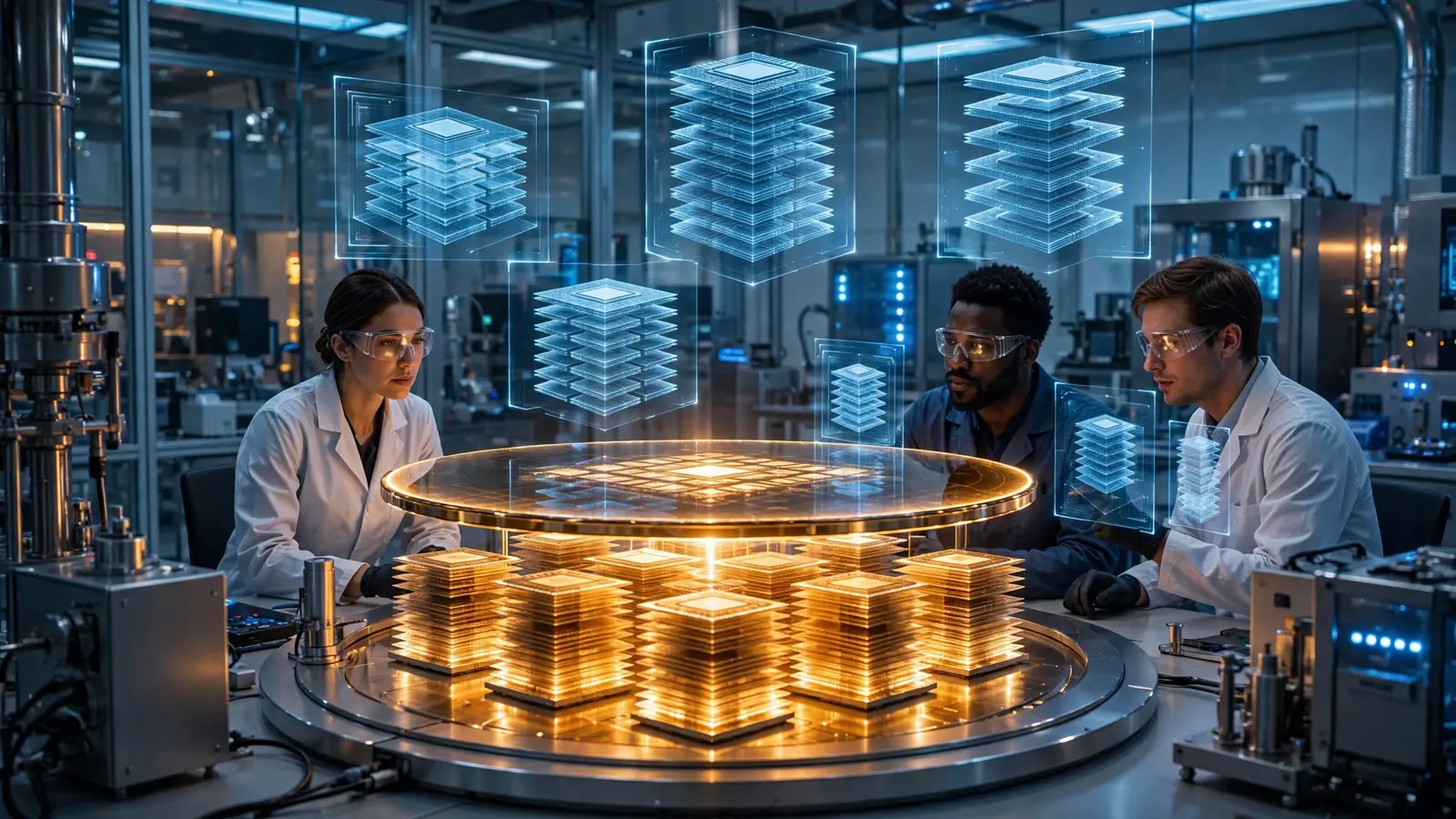
Memory is the wall AI keeps running into. On Tuesday, two of the semiconductor industry's biggest names announced they will attack that wall together: KIOXIA, the world's leading flash-memory supplier, is joining Applied Materials' EPIC Center in Silicon Valley as an innovation partner to develop next-generation memory technologies for the AI era.
Applied Materials, the industry's largest maker of chip-manufacturing equipment, will co-locate KIOXIA's memory engineers inside its $5 billion research campus — the biggest U.S. investment ever in semiconductor-equipment R&D — to work on the cell structures, chip-stacking methods, and materials engineering that will determine how much useful memory AI hardware can pack into a chip.
# Why memory is the bottleneck
GPUs get the headlines, but memory sets the ceiling. Training and running large models is fundamentally a data-movement problem: weights and activations have to travel constantly between storage and compute, and every gigabyte of bandwidth or watt of power lost along the way is capability left on the table.
Applied Materials CEO Gary Dickerson put it bluntly in Tuesday's announcement: “AI infrastructure requires memory solutions that can deliver dramatically higher density, greater bandwidth and improved energy efficiency.” KIOXIA CEO Hiroo Ota framed the bet from the process side, saying the possibilities of memory are “defined by the ability to stretch the boundaries of materials and process innovation.”

# What the partnership actually covers
This is a research partnership, not a product launch — no chips were unveiled. But the four areas the companies named map directly onto how the industry builds more memory into less space:
- Advanced memory cells and structures — new cell designs and physical architectures to push density for AI workloads.
- Multi-chip stacking — integrating memory vertically so density and performance grow within shrinking form factors.
- Advanced packaging — improving integration and interconnect performance in complex multi-die memory solutions.
- Materials engineering — new materials and process approaches that make all of the above manufacturable at scale.
The logic is straightforward: stacking more layers only works if the packaging can connect them and the materials science can build them reliably. By putting the toolmaker and the memory maker in the same building, both sides iterate on the full stack at once.
# Inside the $5 billion EPIC Center
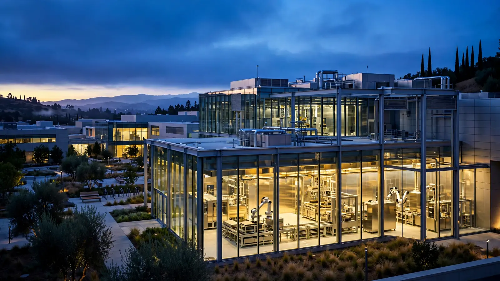
EPIC — short for Equipment and Process Innovation and Commercialization — is Applied Materials' bid to shorten the longest, most expensive part of chip development: the journey from a lab breakthrough to a factory running at scale. The company calls it the largest-ever U.S. investment in advanced semiconductor-equipment R&D, with capital spending expected to scale to roughly $5 billion as customer projects come online. The center is scheduled to be operationally ready this year.
KIOXIA is joining a growing ecosystem there that already includes chipmakers, chip designers, equipment partners, and universities. Chipmakers get earlier access to Applied's R&D portfolio and, the company says, faster cycles of learning; Applied gets a real partner with which to prove its equipment on actual next-generation memory problems.
“Memory is at the center of the AI innovation roadmap,” said Dr. Prabu Raja, president of Applied's Semiconductor Products Group, “and the challenges of increasing memory density while managing cost and complexity require breakthroughs across materials, equipment and process technology.” Minori Kajimoto, KIOXIA's general manager of advanced memory development, said the partnership gives the company “a unique environment to tackle the hardest challenges in next-generation memory.”
# What to watch
Three things will determine whether this partnership matters more than its press release.
First, speed. EPIC's entire pitch is that co-innovation compresses the time from research to high-volume manufacturing. Watch for the first joint technical results — and how long they take to reach a fab line.
Second, the competition. Samsung and SK Hynix dominate the high-bandwidth memory that feeds today's AI accelerators; KIOXIA's strength is NAND flash. The question is how the density and stacking breakthroughs translate into the memory types AI data centers actually buy.
Third, the center itself. A $5 billion shared R&D campus is a new model for the industry — halfway between a national lab and a vendor demo floor. If KIOXIA's move works, expect more memory and chipmakers to take up residence in Silicon Valley's most expensive cleanroom.
Sources
- Applied Materials (via GlobeNewswire) — “Applied Materials and KIOXIA Partner at the EPIC Center to Advance Next-Generation Memory Technology” (September 29, 2026)
- DigitalToday — “Applied Materials, Kioxia launch joint research on AI memory” (September 29, 2026)
- TradingView — GlobeNewswire release mirror (September 29, 2026)